Press Release
Quantum confinement of strongly correlated electrons in artificial oxide structures
October 28, 2011
The University of Tokyo, Japan
High Energy Accelerator Research Organization (KEK), Japan
Japan Science and Technology Agency (JST)
Researchers from the University of Tokyo have succeeded in creating a quantum well structure*1 using strongly correlated oxides, and have for the first time observed the quantized states that demonstrate the confinement of strongly correlated electrons*2 in two-dimensional space. The critical factors for success with quantum confinement were (1) precise growth control of a conductive oxide on an atomic scale using laser molecular beam epitaxy*3 and (2) state-of-the-art spectroscopy using the synchrotron radiation available at the Photon Factory, KEK. Utilizing these growth and characterization techniques, the researchers confirmed that strongly correlated electrons were confined in the quantum well of an artificial oxide structure.
The present result means that the behavior of strongly correlated electrons can be controlled in an artificial two-dimensional space. Strongly correlated electrons confined in two-dimensional space are essential for the emergence of high-temperature superconductivity. Thus, this controllability should allow researchers to develop new superconductors with much higher critical temperatures, hopefully above room temperature, as well as materials having extraordinary functionalities. The successful creation and control of quantum well states in the present study is a first significant step toward creating new electronic devices, as well as controlling the novel physical properties of strongly correlated oxides.
The original report of this work was published on 15 July 2011 in Science.
1. Background
The wide range of properties exhibited by strongly correlated oxides makes them one of the most interesting groups of materials today. High-temperature superconductivity in cuprates is a representative example of the functionality of strongly correlated oxides. Their properties originate in stacked conductive layers, in which strongly correlated electrons are sandwiched by blocking insulating layers (left side of Fig 1). Thus, controlling the behavior of strongly correlated electrons confined in the conductive layers is the key to controlling the extraordinary functionalities of these materials. In fact, it is known that the transition temperature in high-temperature cuprate superconductors increases in proportion to the number of conductive layers sandwiched between two insulating layers. Therefore, it is highly desirable to develop techniques to control the behavior of strongly correlated electrons by using artificial structures.
2. Research Methods and Results
The researchers used laser molecular beam epitaxy to fabricate a quantum well structure based on a strongly correlated conductive oxide of strontium vanadate (SrVO3). The quantum well structure is structurally similar to that of layered complex oxides, as shown in Fig. 1. In the quantum well structure, however, the number of conductive layers can be controlled freely (Fig. 2). The electronic structures of the fabricated quantum well structures were investigated by angle-resolved photoemission spectroscopy*4 using synchrotron radiation at the KEK Photon Factory. The results are shown in Fig. 3. A set of quantization states is observed, providing the evidence for the confinement of strongly correlated electrons in two-dimensional space (conductive oxide layers). As can be seen in Fig. 3(a), the energy positions of the several quasiperiodic peaks evolves as a function of conductive layer thickness: With increasing thickness, one additional peak appears after another, and the peak positions shift to higher binding energies. The spectral behavior is summarized in Fig. 3(b), where the experimental results are compared with theoretical calculations. Fig. 3(b) shows that the experimental data are in good agreement with theoretical predictions, indicating the successful creation and control of quantum well states in artificial oxide structures. Furthermore, additional investigation revealed the existence of other interesting phenomena in the quantum well (Fig. 4): 1) oribital-selective quantization originating from the anisotropic orbital character of the V 3d states and 2) unusual enhancement of the effective mass of the quantized electrons, reflecting complex interactions in the quantum well, neither of which has previously been reported in the conventional quantum well states in noble metals.
3. Research Methods and Results
Using this quantum well structure, it is possible to alter the spin, charge, and orbital degree of freedom of strongly correlated electrons, which could lead to the expression of new physical properties. The successful creation and control of metallic quantum well states in an artificial oxide structure is a first significant step toward creating new physical phenomena and controlling the novel physical properties of such materials, including high-temperature superconductivity. Moreover, we can now look forward to the development of electronics based on strongly correlated oxides, such as superconducting devices and ultrafast optical switching devices.
This work was supported by a Grant-in-Aid for Scientific Research (A19684010 and S22224005) from the Japan Society for the Promotion of Science (JSPS) and the JST PRESTO program. This work at KEK-PF was done under the approval of the Program Advisory Committee (Proposals No. 08S2-003 and No. 09S2-005) at the Institute of Materials Structure Science, KEK.
Publication Title and Authors
“Metallic Quantum Well States in Artificial Structures of Strongly correlated Oxide.”
K. Yoshimatsu, K. Horiba, H. Kumigashira, T. Yoshida, A. Fujimori, and M. Oshima
Science 333, 319 (2011).
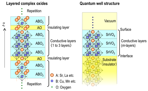
Figure 1. Schematic illustration of the crystal structure of layered complex oxides (left) and the quantum well structure fabricated in this work (right)
Blue and yellow colors indicate conductive and insulating layers. The number of conductive layers in the naturally occurring layered complex oxides is limited to three, while that in the artificial quantum well structures can be controlled freely. It is known that the transition temperature in high-temperature superconductors increases as the number of conductive layers increases.
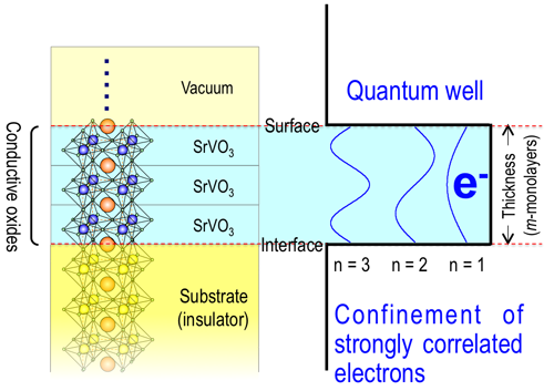
Figure 2. Schematic image of the confinement of strongly correlated electrons in the quantum well structure
Strongly correlated electrons are confined in the conductive oxide layers (a two-dimensional space) sandwiched between the surface (vacuum) and the interface (insulator). The structure is called a quantum well structure. The quantized states can be controlled by increasing the number of conductive layers (expanding the width of the quantum well).
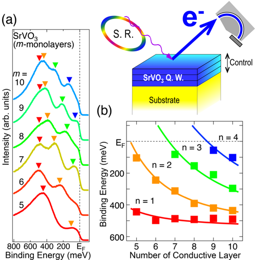
Figure 3. Spectral evidence for the quantum confinement of strongly correlated electrons in artificial oxide structures: (a) Angle-resolved photoemission spectra obtained from the quantum well structure of SrVO3. The peak positions of the quantized states (indicated by filled triangles) systematically change as a function of the number of conductive SrVO3 layers. (b) Plots of the peak positions of the quantization states as a function of the number of conductive layers in SrVO3 (the width of the quantum well structure). Filled squares and solid lines indicate the experimental data and the predictions of theoretical calculations, respectively. The excellent agreement between the two indicates that strongly correlated electrons are confined in the quantum well structure.
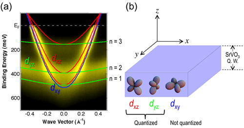
Figure 4. Orbital-selective quantization in the quantum well of SrVO3
(a) Orbital-selective quantization states determined by angle-resolved photoemission spectroscopy. Two types of quantized states are observed. Red and green lines indicate the quantized states derived from dzx and dyz orbitals, respectively. In contrast, dxy states (blue line) are not subject to quantum confinement.
(b) Schematic illustration of orbital-selective quantization. Both dxz and dyz states, whose orbitals expand along the z-direction (perpendicular to the surface), are quantized, while the dxy state, whose orbital extends in the xy-plane (parallel to the surface), is not quantized.
Glossary
*1 Quantum well structure
A quantum well structure is a structure with extremely thin conductive layers (a two-dimensional space) sandwiched by insulating layers. The "well" refers to the shape of the potential energy barrier that confines the electrons and "quantum" means that the width of the well is narrow enough to change the electronic states from continuous to discrete. Electrons can only move parallel to the surface in the quantum well, leading to the formation of digital energy levels in the well. The "quantum well" structure is a key technology in modern electronics and is widely used in devices based on semiconductors such as diode lasers and high-performance transistors for satellite broadcast reception.
*2 Strongly correlated electrons
Electrons can move freely in normal semiconductors and metals. However, when the electron density exceeds some specific value, electrons strongly interact with each other and consequently a unique state appears, where electrons barely move as a group. Electrons in such a state are called strongly correlated electrons. High-temperature cuprate superconductors are representative of oxide materials that have strongly correlated electrons. Oxides having strongly correlated electrons are called strongly correlated oxides.
*3 Laser molecular beam epitaxy
Laser molecular beam epitaxy is a thin film deposition technique in which a high-power pulsed laser beam is focused inside a vacuum chamber to strike a target of the material that is to be deposited. This material is vaporized from the target and the ablated particles (atoms or molecules) from the target are deposited on a substrate as a thin film. This technique is widely used to grow thin oxide films.
*4 Angle-resolved photoemission spectroscopy
Photoelectrons are the electrons emitted from materials appropriately irradiated with light, a phenomenon called the external photoelectric effect. Angle-resolved photoemission spectroscopy is an experimental technique to study the electronic structures (band structure) in materials by measuring the angular dependence of photoemission spectra.
[ Media Contact ]
Hiroshi Kumigashira
The Institute of Materials Structure Science & Condensed Matter Research Center, High Energy Accelerator Research Organization (KEK)
1-1 Oho, Tsukuba, Ibaraki 305-0801, Japan
Tel: 81-29-864-5584, FAX: 81-29-864-5584
E-mail: hiroshi.kumigashira@kek.jp
Tetsuya Ishii
Inclusive Research Administration, Innovation Headquarters, Japan Science and Technology Agency (JST)
Sanbancho-building, 5-3 Sanbancho, Chiyoda-ku, Tokyo 102-0075, Japan
Tel: 81-3-3512-3531, Fax: 81-3-3222-2066
E-mail: crest@jst.go.jp
Ryoji Haraguchi
Research Promotion, Innovation Headquarters, Japan Science and Technology Agency (JST)
Sanbancho-building, 5-3 Sanbancho, Chiyoda-ku, Tokyo 102-0075, Japan
Tel: 81-3-3512-3525, Fax: 81-3-3222-2067
E-mail: presto@jst.go.jp
Yumiko Nagou
Public Relations Office, Graduate School of Engineering and Faculty of Engineering, The University of Tokyo
7-3-1 Hongo, Bunkyo-ku, Tokyo 113-8656, Japan
Tel: 81-3-5841-1790, Fax: 81-3-5841-0529
E-mail: nagoh@pr.t.u-tokyo.ac.jp
Public Relations Office, High Energy Accelerator Research Organization (KEK)
1-1 Oho, Tsukuba, Ibaraki 305-0801, Japan
Tel: 81-29-879-6047 Fax: 81-29-879-6049
E-mail: press@kek.jp
Public Relations and Science Portal, Japan Science and Technology Agency (JST)
5-3 Yonbancho, Chiyoda-ku, Tokyo 102-8666, Japan
Tel: 81-3-5214-8404 Fax: 81-3-5214-8432
E-mail: jstkoho@jst.go.jp
1-1 Oho, Tsukuba, Ibaraki 305-0801 Japan
Copyright (C) KEK. All Rights Reserved.