Press Release
Successful Determination of Silicene Structure Using Reflection High-Energy Positron Diffracion (RHEPD)
December 5, 2013
High Energy Accelerator Research Organization (KEK)
Japan Atomic Energy Agency (JAEA)
The University of Tokyo
The groups of Prof. Toshio Hyodo, Institute of Materials Structure Science, KEK; Dr. Atsuo Kawasuso, Principal Researcher, Advanced Science Research Center, Japan Atomic Energy Agency; and Associate Prof. Iwao Matsuda, The Institute for Solid State Physics, The University of Tokyo studied the structure of silicene, which consists of a single layer of silicon deposited on a single-crystal silver (Ag) surface, using reflection high-energy positron diffraction (RHEPD). This technique can accurately determine atomic positions on the top surface of a crystal. These groups experimentally confirmed for the first time that silicene has an buckling structure unlike planar graphene, which consists of a flat single layer of carbon atoms.
It is thought that silicene has various intriguing properties, and its application to various electronic devices is being explored because it was predicted theoretically that Si atoms in silicene showed slight buckling in the plane unlike planner graphene. However, the buckling structure was not verifired experimentally.
In this study, a single-crystal Ag film comprising 20 atomic layers was grown on a Si (111) surface, subsequent to which Si was deposited onto the surface of the deposited Ag film to form silicene. The RHEPD pattern of the obtained silicene was measured using the world's most intense positron beam with an energy of 10 keV and changing the glancing angle (θ = 0˚–6˚) (Fig. 2).
In this study, first, we analyzed the rocking curve (Fig. 3(a)) measured under the one-beam condition, which is sensitive to atomic coordinates perpendicular to the surface. We confirmed the buckling structure where the distance (Δ) between the upper and the lower layers of Si atoms was 0.83 Å and the distance (d) between Si atoms in the lower layer and the single-crystal Ag surface was 2.14 Å. Then, we analyzed the rocking curve (Fig. 3(b)) measured under the many-beam condition (beam incident from the [112] direction), which is sensitive to atomic coordinates parallel to the surface. The buckling structure was confirmed for two Si–Si bond angles of 112˚ and 119˚ (α, ß), which lead to 4 × 4 symmetry. These results agree well with the theoretical predictions (Δ = 0.78 Å, d = 2.17 Å, α = 110˚, ß = 118˚).
In addition, the experimental results highlight the fact the high-brightness, high-intensity variable-energy positron beam at KEK has sufficient intensity and quality, and is extremely sensitive to atomic geometry on the crystal surface.
Publication:Physical Review B |
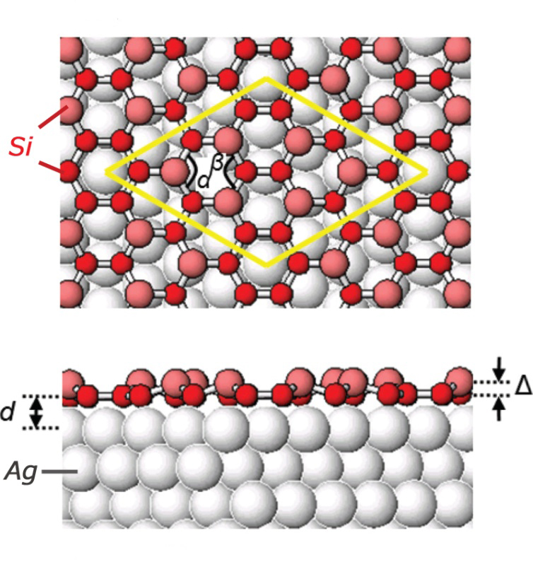
Fig. 1 Structure of silicene on single-crystal Ag surface (Top: plan view; bottom: side view).
Sheet-like crystal of silicon (red, light red) grown on the (111) surface of Ag (gray). The area surrounded by yellow lines shows the unit cell of this crystal. The side view shows that the buckling structure has 6 atoms in the upper level and 12 atoms in the lower level.
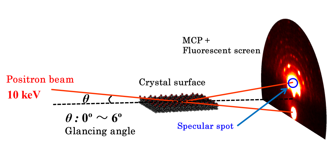
Fig. 2 RHEPD pattern measurement
The positron beam is incident with changing the glancing angle θ, and the contralateral microchannel plate (MCP) detects and amplifies the signal. The resulting pattern appearing on a fluorescent screen in the rear is recorded with a CCD camera.Then the intensity of the specular spot is plotted as a function of θ to obtain a rocking curve.
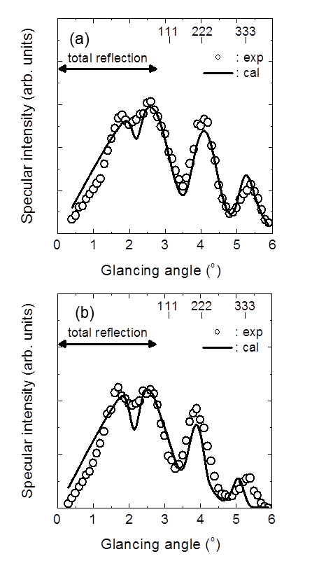
Fig. 3 Rocking curves of the specular spot in RHEPD pattern of silicene deposited on a single-crystal Ag surface under (a) one-beam and (b) many-beam conditions.
Media Contact
[ For Public Relations ]
Public Relations Office, High Energy Accelerator Research Organization (KEK)
TEL: +81-29-879-6046
FAX: +81-29-879-6049
E-mail: press@kek.jp
Public Relations Office, Japan Atomic Energy Agency
TEL: +81-3-3592-2346
FAX: +81-3-5157-1950
1-1 Oho, Tsukuba, Ibaraki 305-0801 Japan
Copyright (C) KEK. All Rights Reserved.