|
|
||||||
| >Top >Feature Story >this page | last update:
09/12/22
|
|
| Detector technology project connects fields It has been almost five years since the launch of the Detector Technology Project (DTP) at KEK. In that time, this new entity has established vital cross-project connections within KEK and beyond, and helped to develop a number of promising new technologies. |
|
||||||||||||||||||
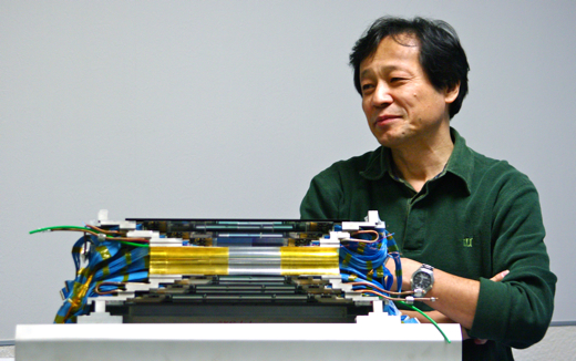
In 2005, Prof. Junji Haba of KEK launched the Detector Technology Project (DTP), receiving a strong support from the then director of Institute of Particle and Nuclear Studies at KEK, Prof. Fumihiko Takasaki (now an Executive Board member). Haba’s goal was to improve the strength of Japan’s detector technologies by establishing a common base for detector development at KEK. This, he thought, would bring about a number of advantages: introduce Japan's frontline technologies to the world, foster cross-disciplinary collaboration, establish domestic bases for technologies critical to sciences using particle beams, and encourage as well as simplify detector research and development activities. “In Japan, detector technologies had been developed on a project-by-project base. The importance of integrating detector technologies and know-how had been neglected,” says the DTP head Haba. “Europe and the US have accumulated knowledge of detector sciences, and have held strong traditions of detector systems.”
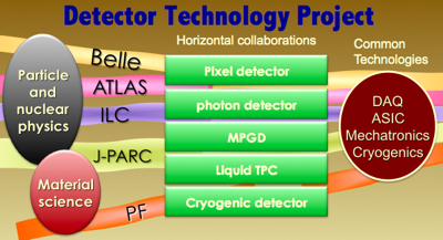
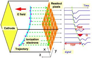
Currently the DTP has seven projects: micro pattern gas detector (MPGD), data acquisition system (DAQ), silicon on insulator (SOI), superconducting tunnel junction device (STJ), liquid time projection chamber (TPC), application specific integrated circuit (ASIC), and photo sensors. “Each project has its own directionality, but each also furthers one or more of our four central goals: to promote applications of detector technology to other disciplines, to lead the world with cutting edge technologies, to establish solid bases for existing technologies which are currently missing or insufficient at KEK, and to promote collective and collaborative research and development activities among universities and research institutes.” Basic principles of particle detection There are hundreds of types of subatomic particles of interest. Such particles include elementary particles like neutrinos, composite particles like B mesons, and force carriers like photons. All of these particles are unimaginably small, and many move very fast. The basic principle of particle detection remains pretty much the same since the very first days of particle detectors. When particles pass through a material, they interact with surroundings either emitting light or knocking electrons loose from the atoms or molecules near the particle's path (ionization). To detect light, scientists use photo sensors. In ionization detection, the electrons knocked loose are carried to sensors by an applied electric field. The information that physicists can derive from these sensors depends on the geometry and capabilities of the sensors. Sensors can collect information about such things as position, the time at which an event occurs, and the number of particles. Readout electronics are generally attached to the rear side of the sensors. These electronics then output the data to computers for analysis. In a nutshell, the basic design of a detector involves choosing the types of the media which particles traverse and ionize, the type of sensor, and the design of the electric readout system. MPGD’s many applications The DTP has already made fruitful contributions to many experiments by bridging multiple disciplines studied at KEK and the Japan Proton Accelerator Research Center (J-PARC). One particularly notable project is the micro pattern gaseous detector (MPGD) project.
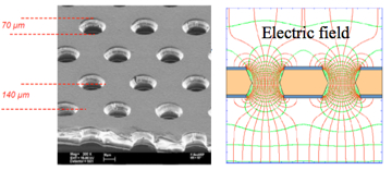
The way to resolve this problem is to amplify the signal electrons. In the vicinity of the sensors, physicists apply an electric field about 100 times stronger than that in the chamber, and accelerate the signal electrons. These electrons become energetic enough to kick out additional electrons from atoms, and those additional electrons are accelerated again to knock out still more electrons from other atoms. When the avalanche of electrons finally hit the sensor, a single electron is amplified to 10,000 electrons. There are several types of MPGDs studied around the world. The MPGD project at KEK studies a type of MPGD known as a gas electron multiplier (GEM). The GEM was first introduced at CERN in 1996. (Another type of MPGD called micromegas is used for the TPC chambers in one of the T2K’s near detectors, which is featured in the article here.) A GEM is essentially a sandwich, with thin copper foil electrodes as the bread, and a polyimide insulator as the meat. Arrays of small holes (around 70 micrometers in diameter) are punched through the sandwich. Lastly, an electric potential of 320 volts is applied across the sandwich, and this voltage is what accelerates the electrons and amplifies the signal. Because each hole on the GEM foil can identify signals, the sensor can report two-dimensional information on one event.
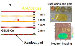
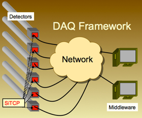
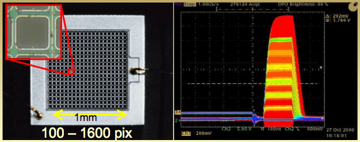
At the J-PARC neutron facility, the use of GEM's has made two-dimensional imaging possible, resulting in better position and time resolution. To detect neutrons, the team coated GEM foils with a neutron-sensitive material, boron. When a neutron hits the boron coating, it produces an alpha particle whose charge triggers the detector signal. The boron coating is inexpensive compared to the very rare isotope of helium (He-3) used for conventional neutron detectors. Also, since boron is sensitive to neutrons but not to gamma rays, it eliminates background noise from gamma rays. Using this technology, the scientists at the neutron facility were able to gain remarkably clear two-dimensional images of the gold content in coins (see image). GEM’s application does not stop there. If coated with X-ray sensitive materials, a GEM becomes an excellent X-ray detector. For example, this can be used to image iron bars deep inside a concrete block, and might bring about a new tool for construction inspection. The collaborators also study applications to medical equipment such as single photon emission computed tomography (SPECT). Standardized electronics KEK’s new data acquisition (DAQ) framework is another notable result of the cross-discipline collaboration fostered by the DTP. The new DAQ was developed by KEK physicist Dr. Tomohisa Uchida, and is now widely being employed. The goal of the DAQ system is to readout data from detectors and send it to a computer as fast as possible.
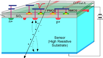
“This way, we do not need individual CPU's inside each detector. All users have to do is to connect the detectors to a hub with Ethernet cables, and they can then start analyzing data in a LabVIEW like environment.” A middleware—computer software tool connecting application software—called robot technology (RT) middleware was specially designed by National Institute of Advanced Industrial Science and Technology to offer user interface to view and analyze the output data. The DAQ-middleware framework brings about almost a plug and play capability. “DAQ-middleware is very useful to small projects that cannot afford a DAQ expert,” says Haba. The SiTPC technology has already found several applications. All GEM detectors developed in MPGD project are equipped with the DAQ. Other applications include Hadron Hall at J-PARC, the neutrino detector Super-Kamiokande, and the CCD readout system for the hyper supreme camera at the National Astronomical Observatory of Japan. SOI: Japan’s leading detector technology Including 70 collaborators, 20 of whom are international, the silicon on insulator (SOI) project is the largest international project in DTP. SOI is a high-resolution, fast and low power sensor currently studied only in Japan. Since 2005, the SOI project has collaborated with Oki Electric Industry, a Japanese company that has strong SOI technology. Ordinary computer chips have a silicon substrate which is several hundreds of micrometers in thickness. Because of the thickness, small parasitic capacitances can form within it, and can degrade the performance of the chip. SOI inserts an insulator between the circuit and the silicon substrate to eliminate the device capacitance, and unnecessary currents flowing in the silicon area. The fast, low current SOI is a widely used technology in the semiconductor industry today.
However, what detector scientists saw in the SOI was not a semiconductor but a sensor. “We can use the silicon as a sensor, and the readout circuit is conveniently attached just 1 micrometers away, completely insulated,” says Haba. “It is an all-in-one technology.” Because the conventional detectors and readout electronics are separate entities, they must be connected by bonding, and the solder bumps for bonding cost at least 50 micrometers of space. With this innovative technology, scientists can skip the bonding, and greatly reduce the amount of material required to construct a sensor. Less material means less disturbance to particle paths, and the better performance in particle physics experiments. Aspiring for unseen energies
The new cosmic microwave background (CMB) radiation group at KEK is in the middle of research and development of an STJ detector to detect primordial gravitational waves in the CMB. A different group, this one led by Prof. Shinhong Kim of Tsukuba University, is seeking a way to detect the neutrino decays thought to occur abundantly in our universe. Through these projects, the STJ may help to answer the most profound questions about our universe. Complete four-dimensional imaging
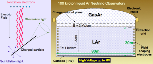
The liquid TPC is vigorously studied in medical research as well. As part of the next-generation positron emission tomography (PET) systems, it will provide much higher resolution images. PET is medical equipment that detects two gammas flying out in opposite directions as the result of electron positron annihilation near cancer cells. The current PET uses scintillator bars of 10 centimeters in length and a few centimeters square cross section, giving special resolution on the order of centimeters. With the liquid TPC, this will be brought down to the order of millimeters or better. As promising as it looks, the challenges are daunting. One major difficulty will be producing the large volume of high quality liquid medium necessary for these applications. The liquid needs to be extremely pure so as not to disturb ionization electrons’ paths. For neutrino experiment, it will require 100 kilotons of liquid argon, all of which needs to be cooled to keep the liquid state. In addition, they need to figure out how to apply one million volts to the container. Catching up to the world Application specific integrated circuits (ASIC) are customized IC chips to be used for a particular purpose. “It is not realistic to mass produce our ICs because we generally need only a small amount,” says Haba. As ICs become smaller and higher performance, it has become difficult to produce ASICs without a well-established infrastructure. “Europe and the US have long put efforts on ASIC development, while Japan has put less focus on the matter.” The ASIC project aims to train ASIC developers beyond KEK at universities around Japan. The project has hosted ASIC programs to promote in-house ASICs. Now scientists at universities such as the University of Tokyo, Kyoto University, Saga University, and Tohoku University who have completed the program can fabricate detector readout systems on their own. At KEK as well, the team has developed ASICs for both the MPGD and liquid TPC. Strengths of research and development community The next-generation photo sensor project is the second largest project in DTP, and includes over 60 collaborators from various projects such as T2K, the International Linear Collider (ILC), and Belle. The project’s main interest has been the multi pixel photon counter, MPPC, developed by Hamamatsu.
The R&D activities proved to be useful experiences for collaborators from other projects. MPPC studies for ILC and Belle are ongoing. “The first generation of MPPCs has been completed,” says Haba. “However, there are some disadvantages of MPPCs that need to be overcome for the next application. For example, you cannot make the pixel much larger than the order of 1-millimeter square as the noise grows steeply with the size.” The team is currently exploring various options to overcome these problems. Growing into the future The DTP has grown to attract more than 260 collaborators. “Our primary goal to build a pipeline between projects has been accomplished,” says Haba. “Also, the project provides a place where detector scientists can work on R&D of detector technologies not directly related to experiments at KEK.”
Haba thinks that there is a room for improvement in terms of communication. “For wide variety of scientists at KEK, we’d like to improve the quality of seminars and offer places to discuss new technologies more casually.” The DTP project welcomes new collaborators. |
| copyright (c) 2009, HIGH ENERGY ACCELERATOR RESEARCH ORGANIZATION, KEK 1-1 Oho, Tsukuba, Ibaraki 305-0801 Japan |
||