|
|
||||||
| >Top >Feature Story >this page | last update:
10/07/14
|
|
| An advanced 2D detector for medical, materials and life sciences One of the Detector Technology Project (DTP) groups at KEK has developed multi-purpose, two-dimensional detector called a gas electron multiplier (GEM) for use in small radiation-related experiments. The GEM’s good time- resolution has also given birth to a new field of radiography, called energy- selective radiography. Read here how GEM can play an important role in neutron science, medical applications, and more. |
|
||||||||||||||
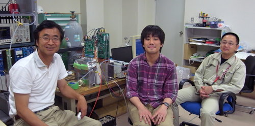
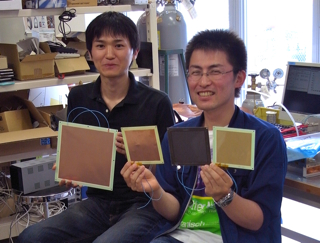
For Kohichi Miyama, a graduate student at Tokyo University of Agriculture and Technology, particle detectors are brilliant tools to see the unseen using the power of science. As an undergraduate, he worked on gas chamber, detecting tiny charged particles with detector called a gas electron multiplier (GEM). Now, his passion is to do something practical using particle detectors, something that helps to improve our lives. His short-term goal: to develop a high-precision gamma-camera. A year ago, Miyama joined Takahisa Koike of the International University of Health and Welfare, who is applying GEM to gamma-camera medical imaging.
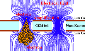
“Traditionally at KEK, particle and nuclear experimentalists are very keen in the field of advanced detector technology developments, but previously did not actively share their expertise with researchers in other disciplines. Small-scale experiments such as those in materials science and the life sciences rarely had access to cutting-edge technologies,” says Uno. “The idea of the MPGD project at DTP is to develop a high-quality GEM that is easily accessible to non detector experts.” The GEM, incorporated with the general-purpose data acquisition system (DAQ) developed by the DAQ project in DTP, has the potential to detect many types of ionizing radiation such as neutrons, X-rays, charged particles, and ultraviolet light. Flexible geometry and multi-purpose detector GEM is a gaseous ionization detector, in which incoming particles ionize the gas inside the chamber, producing electrons. An essential feature of all gaseous ionization detectors is the amplification of the resulting electrons by a factor of millions or more. The amplification depends on the application of a high voltage. Without amplification, sensors are not sensitive enough to detect the initial small electron signals. For example, in a wire chamber, a high voltage is applied to sense wires that run the length of the chamber.
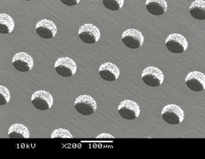
An interesting feature of the GEM is that scientists can readily change the type of particles detected, by introducing several layers of converter GEM foil coated with different types of metal. Incoming ionizing particles interact with the metal coating, producing electrons, which are accelerated through the holes. The electrons from these converter GEM foils are then amplified at the final GEM layer before readout. For neutron detection, scientists apply a coating of boron-10 to the converter GEM foil, so that when incoming neutrons hit the boron, the ionizing particles that are produced are alpha particles. For X-ray detection, gold is the X-ray sensitive material used to coat the converter GEM foil. GEM’s advantages are many. First, the geometry of the GEM is flexible. Each hole in the GEM foil can detect and amplify a signal. This means that the detector, together with the flexible geometry of the readout pad, can report two-dimensional information of any desired shape. Second, the background noise is generally low. The coating material is chosen to be specifically sensitive to one type of particle. For example, boron is sensitive to neutrons but not to gamma rays, which eliminates background noise from gamma rays. Third, the manufacturing and mass-production of GEM is easy compared to chambers that require intensive hand labor to produce. KEK’s all-in-one GEM Uno’s ambition was to use existing technologies to make advanced detectors readily available for a wide range of experiments. For those investigators who cannot afford to spend significant effort on detector development, it is best that detectors be up and running as soon as they are installed. This is a challenging thing to do. First, detectors must be sensitive to the right type of particles, in the right range of energies, and with the desired resolution. Second, the signals need be collected and converted to the right format for storage, a process that depends on the type of experiment. Finally, the detectors need be monitored for continued good performance. In order to work, detectors must have well integrated hardware and software that work smoothly together for seamless data acquisition, or DAQ.
Experiments in materials science generally have limited room for detector and readout electronics. What was needed was a simple, cost-effective, and compact readout system. “Compact detectors also bring about many applications in other disciplines such as medical and non-destructive testing,” says Dr. Tomohisa Uchida of KEK, the leader of the DAQ group, who developed the readout system for GEM.Uchida developed compact electronics boards that are integrated with the GEM detector and that can transmit data to PCs via the standard Internet transmission protocol (TCP). Combined with the DAQ-Middleware also developed by the DAQ project members, the final GEM system is now an all-in-one detector system. The ideal solution for a neutron detector The most natural target of the GEM application is the neutron experiments now starting at the Japan Proton Accelerator Complex (J-PARC). “Neutrons are the easiest target particle for the GEM, because the ionizing alpha particles produced when neutrons hit the boron coating are very effective ionizers that can produce many electrons,” says Dr. Hidetoshi Ohshita of KEK who is in charge of detectors at one of the neutron beamlines at J-PARC, NOVA. In particular, GEM has a relatively low detection efficiency due to its low capture rate. That makes it an ideal detector for the neutron beam monitor, which is supposed to absorb only a very small fraction of the incoming beam. “This shortcoming of GEM is actually an advantage for our purpose.”
The GEM is a strong candidate for the future neutron detector at J-PARC’s neutron beamlines as well as being used in monitors. “Helium-3 wire detectors are generally used for neutron detectors. They are very sensitive to neutrons and have very high performance, but it’s been pointed out that they may not survive the neutron intensity that is expected when the J-PARC accelerator reaches its full power at one megawatt,” says Uno. The GEM has a very high tolerance to beam intensity, and has particularly good time-resolution so that it can measure the incoming neutron energy very precisely by the time-of-flight method. In addition, GEM gives two-dimensional information with good spatial resolution, which is not possible with a one-dimensional wire chamber. To use GEM in neutron detectors, however, the team first needs to overcome GEM’s low detection efficiency. They are now testing various ideas to improve the efficiency. “The boron layers in the GEM detector are not meant to amplify signals, so they need not be GEM foils. We are investigating what other neutron-sensitive layers can produce higher efficiency for neutron detection,” says Uno. If the scheme turns out well, this will be a big step forward for neutron experiments.
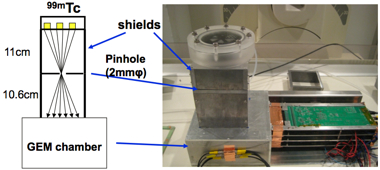
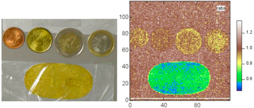
A new field: 2D neutron imaging A particularly interesting spinoff of the GEM appeared in the new field of neutron radiography. The flexible geometry of the GEM makes possible the complete two-dimensional imaging of an object’s composition. Take a look at the neutron image of various coins. The difference in the gold content of Euro coins and the Japanese oval gold coin from the Edo period is unmistakably clear. “The different compositions are distinguishable when the sensor can measure the neutron energy with precision. Imaging like this is only possible when we have a pulsed neutron beam and 2D detectors with very good time-resolution,” says Uno. “GEM happens to have those capabilities.”
“There have recently been rapid developments in two-dimensional energy-selective radiography, demonstrating successful imaging of many types of samples,” says Uno. “The limit of its applications, we don’t yet know. We are investigating its potential.” Many applications of gamma-ray imaging GEM is so adaptable because changing the type of metal coating can make it sensitive to other particles, such as photons. To detect gamma rays, the boron coating in a neutron-detecting GEM is replaced by a gold coating. The usual photon detectors employ scintillator crystals that are generally very expensive. GEM offers an inexpensive alternative. Further, crystals are not easily made small, and each requires one readout channel. GEM and its readout pad have flexible geometry, and are at an advantage for a high two-dimensional spatial resolution.
GEM for the future of 2D imaging With many interested researchers from universities and research institutes throughout the country, the GEM’s potential is only growing. For example, for the use of GEM in X-ray imaging, a graduate student from Shinshu University, Takuya Fujiwara, has just joined the team to study how to improve the detection efficiency. He plans to use a two-sided electronic readout board for the next beam test to see how this will boost detector performance. Aside from the gamma-camera imaging that Koike and Miyama study, the GEM also has the potential to be used in positron emission tomography (PET). Potential GEM applications are being investigated at Hokkaido University, the Photon Factory at KEK, neutron and muon beamlines at J-PARC, and others. “I see a very big potential in the GEM. Many researchers find uses for the detector, and we simply provide the detector for them to study using their own setups,” says Uno. “The GEM has wings now.” |
| copyright (c) 2010, HIGH ENERGY ACCELERATOR RESEARCH ORGANIZATION, KEK 1-1 Oho, Tsukuba, Ibaraki 305-0801 Japan |
||