|
International collaboration at KEKB 2008.9.29 ■CesrTA project at Cornell University (1) Electron clearing electrode R&D
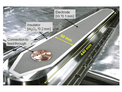
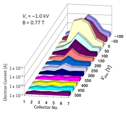
One of the most important problems faced by advanced positron/proton storage rings is the electron-cloud effect. A direct and efficient method to solve the problem is the installation of a clearing electrode into the beam pipe. A thin strip-line clearing electrode was developed and recently tested using the KEKB positron ring [1]. The electrode is composed of a thin metal layer formed on a thin dielectric layer, as shown in Fig. 1. The narrow alumina gap between the electrode and the beam pipe decreases the beam impedance, and also enhances the heat transfer from the electrode to the beam pipe. A test chamber with the electrode and an electron monitor to measure the electron number inside was installed into a wiggler magnet with a vertical field intensity of 0.77 T. Figure 2 shows an example of the horizontal distribution of electron numbers while changing the electrode voltage (Velec) from -100 to +500 V on the logarithmic scale. The reduction ratio around the beam orbit (Collector No. 4) was approximately 1/100 for Velec = +300 V. The results experimentally demonstrated the feasibility of a clearing electrode for intense positron rings. This electrode is well available to the positron damping ring (DR) of International Linear Collider (ILC), where the electron cloud problem is a crucial issue. The collaborative experiment using a clearing electrode based on our design was incorporated into the CESR-TA program ongoing in Cornell University for the R&D of ILC DR.
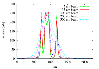
(2) X-Ray beam profile monitor R&D The goal of this R&D collaboration between KEK, Cornell University and the University of Hawaii is to develop a wideband, high-speed x-ray monitor for beam profile measurements for high-resolution, bunch-by-bunch measurements. The optics being tested are based on the principle of coded aperture imaging. Coded aperture imaging is a technique borrowed from x-ray astronomy wherein an array of pinholes (the coded aperture) is used to create a coded image of the source, which can then be decoded using the known aperture pattern to reconstruct the original source image. This approach combines the resolution of a pinhole camera with open apertures of up to 50% to maximize the detected flux, which in turn minimizes the integration time needed to image the beam. A prototype mask has been fabricated and is undergoing testing at CesrTA, an ILC damping ring test accelerator at Cornell. The mask and simulated detector images for various beam sizes are shown in the accompanying figure. Development is also proceeding on high-speed readout methods.
YS & JF:mn web-acc at ml.post.kek.jp |