|
|
||||||
| >Top >Feature Story >this page | last update:
10/03/30
|
|
| Thriving new detector technology: SOIPIX On March 4-5, 2010, KEK’s detector scientists and international collaborators from around the world gathered in a meeting room at Fermilab to discuss a new detector technology: silicon-on-insulator pixel (SOIPIX). Learn about KEK’s new technological endeavor, and the recent steps made by collaborators to make this powerful new technology work. |
|
|||||||||||||||||||||
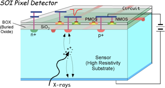
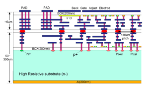
For detector scientists, this new technology may be revolutionary, changing the way some types of the particle and photon sensors are fabricated (or built). The technology is called silicon-on-insulator pixel or SOIPIX. This innovative technology is starting to draw attention from the world detector technology community for its high speed, high spatial resolution, low power consumption, and compactness. In general, detecting particles or photons requires two devices: a sensor, and it's associated readout electronics. For a silicon sensor, detector scientists conventionally use services of semiconductor companies specialized in processing of devices on high resistivity substrates. For the electronics to be connected to the detector, integrated circuit technology called complementary metal-oxide semiconductor (CMOS) is commonly used. Interactions of particles or photons in silicon sensor produce secondary electrons and electron holes. These secondary electrons and holes are converted into a voltage pulse, which is then amplified to produce a usable signal. When constructed with conventional CMOS technology, these two components (readout electronics and sensor) are produced separately, and then mechanically bonded by a technique called bump-bonding. In SOI, the two parts are produced together on a single chip. Only an insulating layer of sub-micron in thickness separates the readout electronics part and its silicon substrate. The ingenuity of the detector scientists is that they use the silicon substrate as the sensor.
For the detector, SOI provides many more advantages. First, because of the very thin substrate (~40 nm) of the electronics part, the electronics are affected less by charges produced by radiation in the substrate. The radiation hardness is particularly important for use in particle accelerator and in space. Second, SOI transistors can tolerate a broad range of temperatures compared to standard CMOS technology. This makes them convenient for use in extreme conditions such as in space. Third, because of the insulator between pixels, each pixel is electrically less affected by the neighboring pixels. This means that pixel size can be reduced, improving spatial resolution dramatically. Finally, the thickness of the sensor can be adjusted. This means that the sensor can be made as thick or thin as desired, as long as the appropriate amount of voltage can be applied to it for particle detection. Pixel detectors using SOI technology can provide an ideal detector for high energy particles, and photons X-rays up to a dozen or so keV.
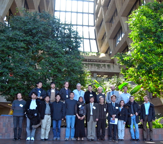
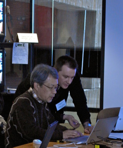
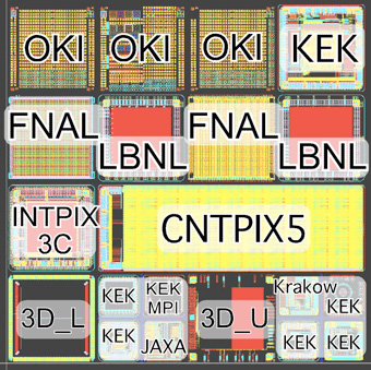
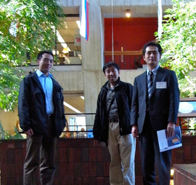
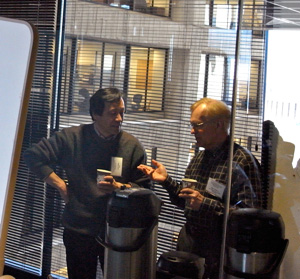
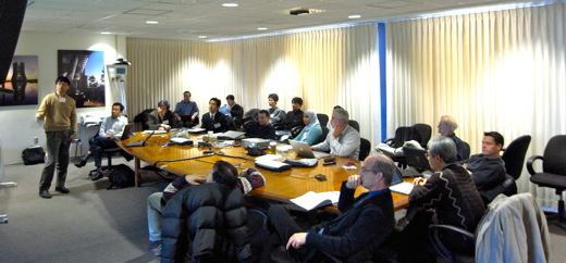
Open SOIPIX collaboration The idea of using SOI technology for a particle detector is also not new. It has been around for a decade. European scientists started investigating the technology some time ago, but they soon abandoned the idea because the semiconductor technology they were using did not give the desired results. Later, in 2005, the idea was picked up by Prof. Yasuo Arai at KEK, the leader of the SOI group in the KEK Detector Technology Project (DTP). He saw vibrant opportunity in the technology, an opportunity to bring cutting-edge technology to the world, technology from Japan. “As I researched the SOI technology, I found out that Japan had a very strong technological background in SOI,” says Arai. “The detector had enormous potential that was not fully explored, and yet the problems were tractable using the advanced semiconductor processing technology we had in our country.” Arai’s strategy was to make the SOIPIX processes they developed open to everyone. “Openness invites competition, and brings about rapid advancement in SOIPIX technology,” says Arai. He called for collaborations overseas, and now the SOIPIX group is the best funded and largest international group among the eight DTP projects at KEK. In 2006, the team was joined by several US laboratories, including Fermilab, Lawrence Berkeley National Laboratory (LBNL), and University of Hawaii. More recently, they have also been joined by several institutions from Europe. SOIPIX collaboration meets at Fermilab The SOIPIX collaboration now has around 100 member scientists from 16 institutions. The 5th collaboration meeting was held at Fermilab on 4-5 March of this year, and was the first formal SOI meeting held outside Japan. Around 30 participants from 10 research institutions attended. Participants came from Belgium, Italy, Japan, Poland, and US, and from two Japanese companies: OKI Semiconductor Co. Ltd. (OKI Semiconductor) and ZyCube Co. Ltd. (ZyCube). While most attendees were present on-site, some attended via remote link. All enjoyed intense discussions on their new results.
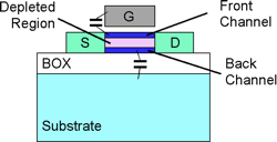
Making it work—a challenge of back-gate problem SOI has a layer of buried silicon oxide as an insulator between the electronics and the substrate. For commercial use, this is all that is needed for an SOI device, because the only component of interest is the electronics.
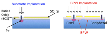
The problem with the back-gate effect is that the voltage rise can cause the transistor to turn on, which would cause the pixel to no longer work. The effect imposes an upper limit of 10 to 15 volts on the back of the substrate, which in turn limits the thickness of the depletion region. In discussion with OKI Semiconductor engineers, Arai and his team came up with a solution to the back-gate problem. The solution was to add buried p-wells (BPWs) to the detector. Arai and his team implanted boron ions into the silicon around the pixel right beneath the buried oxide. The tungsten plug can then be used to control the voltage of the boron well, and therefore the voltage beneath the transistors. This solves the back-gate problem.
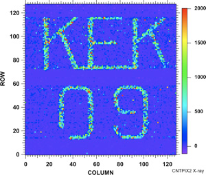
The result of the BPW test was remarkable. This modification raised the maximum substrate bias voltage to above 130 volts. The team further found that using the boron implantation method also reduces the pixel size and improves radiation hardness. The functioning of an SOI detector with BPW technology was proven in Japan a year ago, and has since been investigated for SOI detectors by other groups worldwide. At the recent SOIPIX collaboration meeting, groups from Institute of Nuclear Physics at Krakow (Poland), Lawrence Berkeley National Laboratory (LBNL), and Fermilab all reported separate results showing that the BPW solution gave successful results.
OKI semiconductor’s presence in SOI OKI Electric Industry Co., Ltd. was the only company in the world that mass-produces fully-depleted type SOI chips. When Arai started out with his project, there was an important prerequisite to gain OKI’s cooperation for the idea of an SOI detector. “Without industry cooperation, our project cannot exist,” says Arai. For OKI as well, SOI’s high price range demanded applications beyond mass use. A detector for high energy physics may be just such application. The two parties found they had common interests. The partnership continued even after OKI’s electronics division was taken over by Rohm Co. Ltd. in 2008 to form OKI Semiconductor Co., Ltd. In fact, the partnership grew even stronger. “It took some convincing,” recalls Arai. He and his colleagues from overseas visited the company and successfully argued that pursuit of academic interests has significance, and that there is great potential in SOI beyond Japan and beyond high energy physics.
The demand for OKI Semiconductor’s SOI processes is high, and is gathering great interest from new SOIPIX collaboration members as well. Lawrence Soung Yee, a PhD student from the Université Catholique de Louvain in Belgium, has been investigating the SOI process using the university’s in-house technology. He says: “For the next generation we are thinking OKI Semiconductor technology. It is more advanced technology than what we have right now.” SOIPIX’s new direction—vertical integration An exciting recent development in SOIPIX is the 3D integration of circuits. “Vertical integration can remove some of the problems that are associated with SOIPIX processes, by decoupling the sensor and readout processes,” says the head of the ASIC Development Group at Fermilab, Dr. Raymond Yarema. “The 3D technology uses new ideas about how to create connections between sensors and readout electronics. This allows lower mass components and lower cost connections between the sensor and the readout electronics.”
Efforts in vertical integration are facilitated by institutions from Europe, the US, and Japan. KEK and Fermilab play central roles. “A consortium of parties interested in vertical integration was initiated by Fermilab and now involves 16 institutions. This is about the same size as the SOIPIX collaboration. We pursue somewhat different approaches and applications,” says Yarema. The consortium is exploring applications for such experiments as the LHC, the B Factory in Italy, and new light sources. One big step forward When Arai started advertizing the project oversea, US institutions were the first to join the collaboration. Since then, many institutions from countries in Europe and Asia, as well as from other disciplines such as astronomical observatories within Japan, have expressed interest.
In his concluding remarks, Yarema said: “The analysis leading to the nested buried well concept, and ideas beyond this, show that there is much to explore in future runs, and that this should lead to many interesting talks at future meetings.” The head of KEK DTP, Prof. Junji Haba, was also present. “KEK has a strong interest in pursuing the SOI detector technology. The flank discussions held at the meeting between industry and oversea project groups will certainly motivate the advancement of the technology.” Arai’s goal: to increase the proportion of SOI designs submitted by oversea institutes. Right now, KEK takes up about a half. The next set of submissions will be this summer.
|
| copyright (c) 2010, HIGH ENERGY ACCELERATOR RESEARCH ORGANIZATION, KEK 1-1 Oho, Tsukuba, Ibaraki 305-0801 Japan |
||