
Font size 

Advanced Studies

Accl. Operations

Past Accl. Operations
Accelerator R&D

Theoretical Research
Archives
Completion of the First Production Version of the Accelerating Cavity for the SuperKEKB Positron Damping Ring
A positron damping-ring accelerator (hereinafter called the “DR”) is under construction to fulfill the requirement for the low-emittance positron-beam injection into the main ring of the SuperKEKB accelerator which is based on the nano-beam scheme. We have developed a radiofrequency (RF) accelerating cavity (hereinafter simply referred to as “the cavity”) for the DR. The cavity is an evacuated metal resonator, into which we input high-power RF waves to excite an electromagnetic mode with a high electric field to accelerate charged particles. We usually use copper to make such cavities because of its high electrical and thermal conductivities. The cavity in the present work is mainly made of high-purity oxygen-free copper (class1). In the following, we refer to this cavity as the “DR cavity.”
We designed the DR cavity based on the higher-order-mode (HOM) damped structure of the normal-conducting RF accelerating cavity system called “ARES” (Accelerator Resonantly coupled with Energy Storage), where the ARES cavity system (hereinafter simply referred to as “the ARES”) is made of three electromagnetically coupled cavities: an accelerating cavity, an energy-storage cavity and a coupling cavity as an in-between one. We have successfully operated 32 sets of the ARES at the KEKB main rings with extremely low trip rates. Since the accelerating-mode frequency is the same as used in the KEKB main rings (508.887 MHz), the basic structure of the DR cavity is the same as that of the accelerating cavity in the ARES. However, no coupling or energy-storage cavities are used, just an accelerating cavity (single cell). The accelerating voltage per cavity (hereinafter called the “cavity voltage”) in the ARES is 0.5 MV in specification. Previously, the required total voltage in the initial DR design was 0.26 MV, meaning that one cavity was enough for DR accelerator operation. However, it was shown theoretically that single-bunch instabilities caused by coherent synchrotron radiation would significantly affect the operation if such a total voltage was used. Now, a total voltage of 1.4 MV is required but the theoretical uncertainty is still large. It should be noted that 1.4 MV is required as per the DR design specifications, and the hardware (cavity) performance should exceed this requirement. In order to supply a voltage higher than 1.4 MV to the DR in a space originally designed for one cavity, we have proposed and developed an RF accelerating structure that can accommodate up to three cavities, as shown in Figure 1. In this structure, each cavity body (shown in Figure 2) is mounted with an input coupler, a movable tuner, HOM waveguide loads, and a vacuum evacuation system. We will assemble the cavities, separating them with grooved beam pipes, similar to LEGO blocks. We chose the cavity voltage in specification of the DR cavity to be 0.8 MV, higher than that of the ARES cavity (0.5 MV), guaranteeing a supply of 1.6 MV to the DR with two cavities (higher than the requirement of 1.4 MV), or 2.4 MV with three cavities. In the two-cavity configuration, a dummy duct is used in place of the middle cavity.
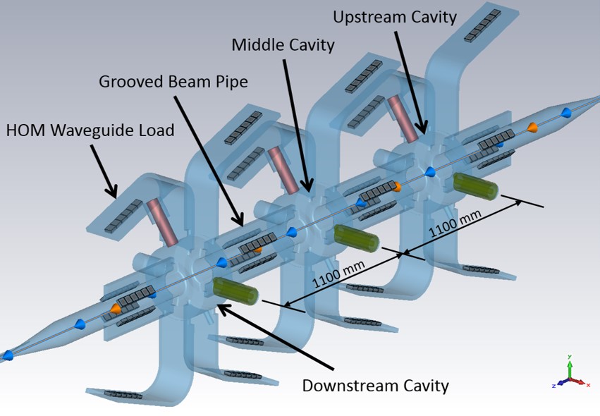 |
| < Figure 1 > Conceptual diagram of the accelerating structure. The blue, gray, green, and magenta regions indicate the vacuum, HOM absorbers, coaxial lines of input couplers, and plungers of movable tuners, respectively. The colored arrows indicate the direction of the positron beam. |
|
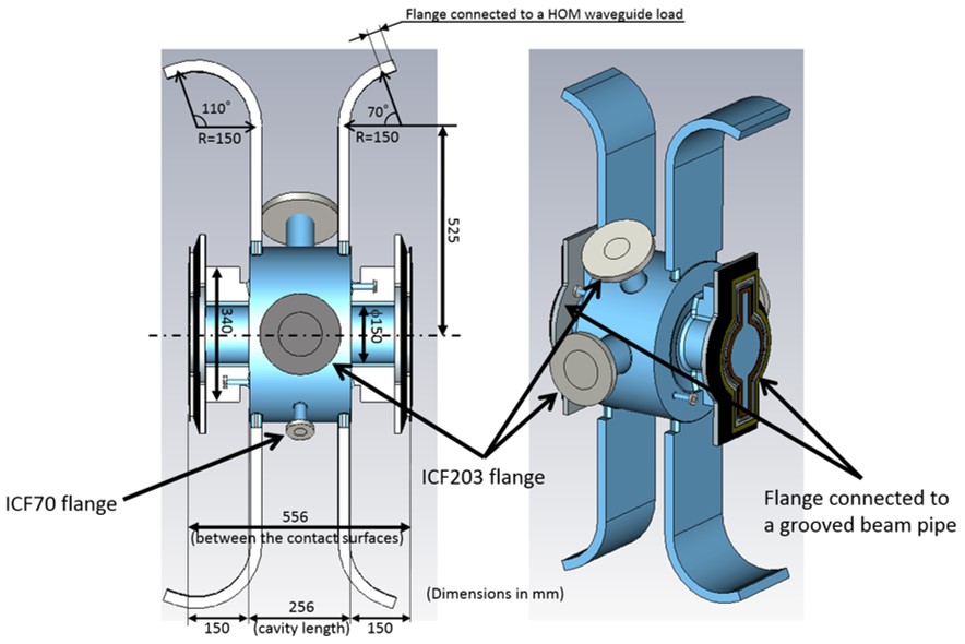
| < Figure 2> Conceptual diagram of the main body of the DR cavity (single cell). The blue region indicates the vacuum. |
Apart from the coupling and energy-storage cavities, the DR cavity has the following space saving features that are not included in the ARES:
1. The HOM absorbers are all compact tile-shaped silicon carbide (SiC) ceramics, as shown in Figure 3 (whereas large bullet-shaped SiC ceramics were used for the HOM waveguide loads in the ARES).
2. The grooved beam pipes are made common between the neighboring cavities, extracting and damping horizontally polarized dipole modes out of harmful HOMs generated in the neighboring cavities when charged particles pass through them.
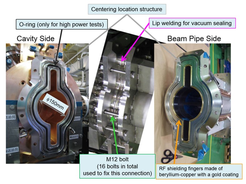
3. The cavity is connected directly to grooved beam pipes with lip welding for vacuum sealing at the outer periphery (technically known as a “weld ring gasket”). It also includes RF shielding fingers and a centering location structure, as shown in Figure 4.
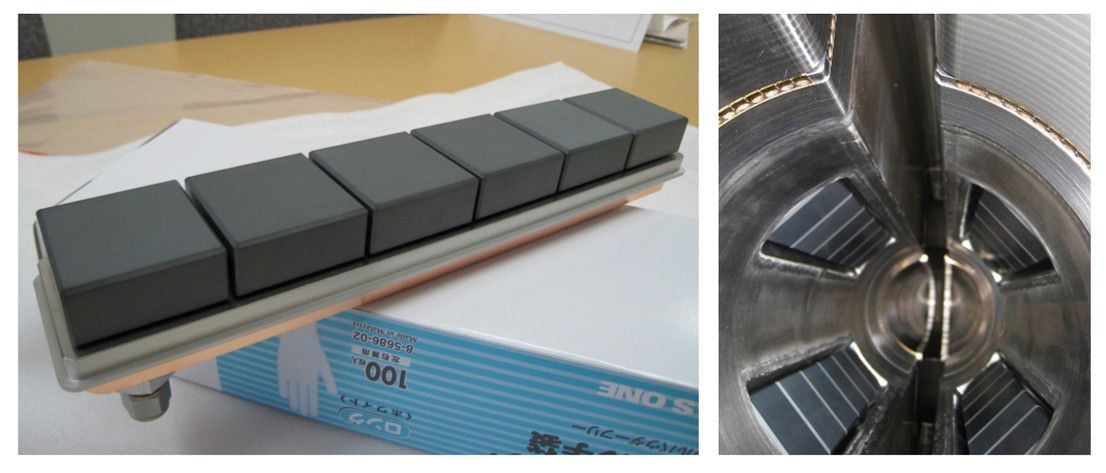 |
| < Figure 3 >The left photograph shows one set of six SiC tiles brazed on a copper cooling plate. The right photograph shows the inside of a grooved beam pipe loaded with four such sets of SiC tiles. |
|
| < Figure 4 > Connection between the cavity and grooved beam pipe. |
In this accelerating structure, all of the related HOMs are damped, including those moving between the cavities, so that the electromagnetic field in each cavity has high independence. Furthermore, the number of cavities used in this accelerating structure is variable, yet it can still be considered a single mechanical structure with solid connections between the components (cavities, grooved beam pipes, etc.). This “multi single cell” design is the most significant characteristic of this structure.
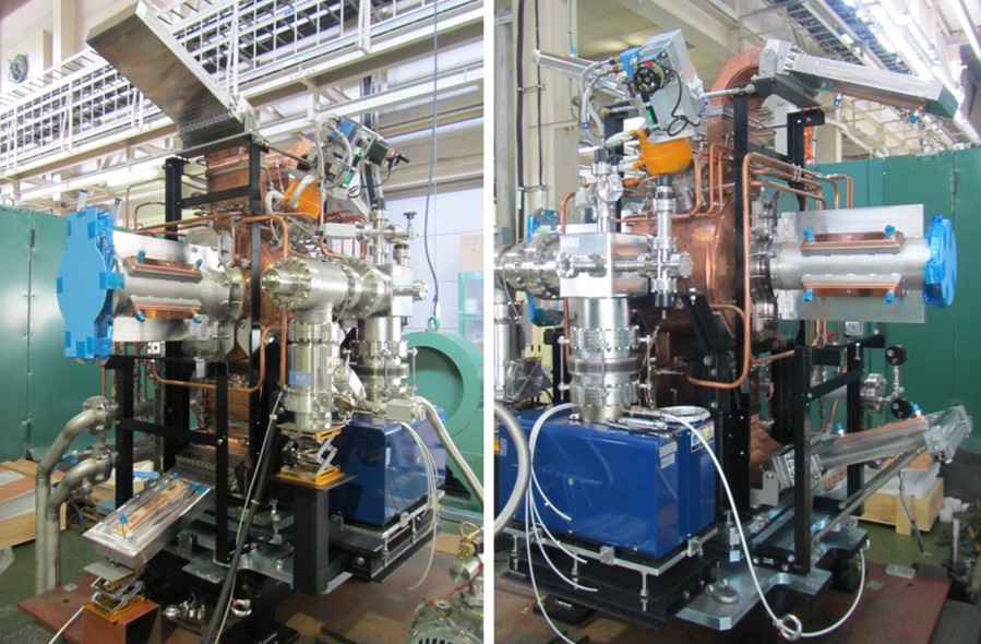
We constructed a prototype cavity in fiscal 2011, and performed a high power test in fiscal 2012. Using the results of the prototype, we constructed the first production-version cavity (hereafter referred to as “cavity No.1”) in fiscal 2012, and performed a high power test in June and July of this year. Its setup is shown in Figure 5. In this test, no charged particles were injected into the cavity from the outside; however, X-ray radiation was generated when field-emitted electrons from the inner surface of the cavity accelerated and impacted the opposite inner surface. Therefore, this test was performed in a radiation controlled area.
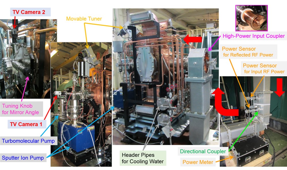 |
< Figure 5 > High power test setup for cavity No.1. The red arrows indicate the flow of high power RF waves coming from a klystron through the waveguide into the cavity. In this test, no HOM waveguides or grooved beam pipes were mounted. |
There are several small differences between the prototype and cavity No.1; however, there is only one significant difference related to the high-power RF performance, which is the application of electro-polishing (EP) in the production process. The inner surface of the prototype was protected with acid cleaning followed by chromating. In cavity No.1, the inner surfaces of the endplates to be exposed to high RF fields were electro-polished with about 40 μm of etching instead of the acid cleaning followed by chromating. As shown in Figure 6, EP achieved a mirror-like surface. Because there is only one such difference between the prototype and cavity No.1 related to the high-power RF performance (the EP), we can experimentally evaluate EP efficacy on normal-conducting RF accelerating cavities in the UHF band of continuous waves by comparing the test results of the two cavities.
Before high power tests, we usually perform low power tests, using a network analyzer, to ensure that the cavity has been made as designed. First, we measured the accelerating-mode frequency (508.887 MHz in the design), which is the most important quantity. The result was in excellent agreement with the prediction of our numerical simulation; the difference was just 0.02% for cavity No.1. The unloaded quality factor (hereinafter denoted by “Q0”) is also an import dimensionless quantity (about 30000 in the case of the DR cavity) because the acceleration efficiency becomes higher with higher Q0. Q0 of the prototype was measured to be 93% of the theoretical value calculated for an ideal cavity. Q0 of cavity No.1, however, was improved to 97%. Finding no problems with the above results or with the other measured quantities, we proceeded to the high power test.
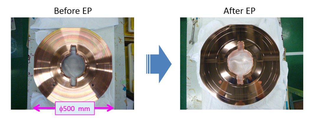 |
| < Figure 6 > Photographs of the endplate of cavity No.1 before (left) and after (right) electro-polishing (EP). Through EP, the average surface roughness (Ra) was improved from about 1.5 μm to about 0.2 μm. In the right photograph, the surface is so smooth that the photographer‘s arms are clearly seen. |
Figure 7 (right) shows the aging history of cavity No.1. The cavity voltage reached 0.9 MV without any problems, exceeding the cavity voltage required by the specifications (0.8 MV). Also shown in Figure 7 (left) is the aging history of the prototype for comparison, revealing that cavity No.1 has the following advantages:
(a) Lower vacuum pressure (i.e. better vacuum)
(b) Lower trip rate
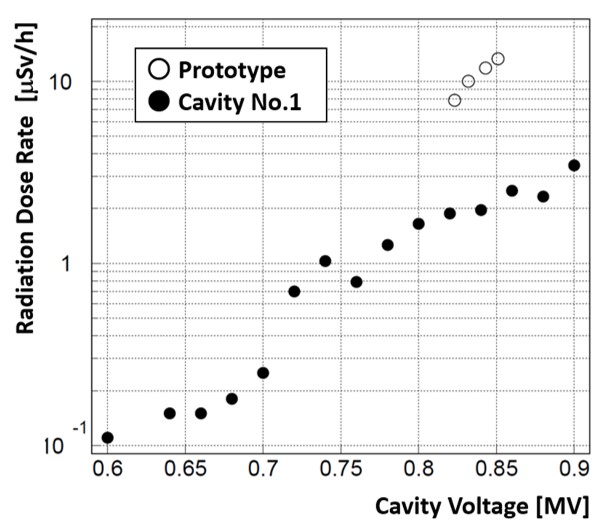
(c) Lower radiation dose rate as shown in Figure 8 (about one fifth), meaning that there were fewer field-emitted electrons with the same cavity voltage
It should be emphasized that all of the above advantages, the higher value of Q0 and (a)-(c), are a result of EP. It should also be noted that we could not make a simple comparison between the times taken to reach 0.9 MV because of the different aging parameters in the computer controls.
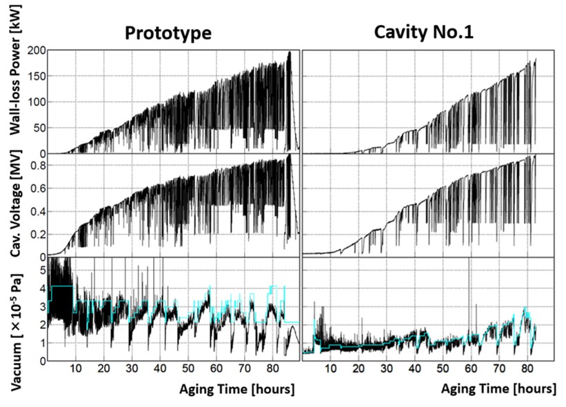 |
| < Figure 7 > Aging histories of the prototype (left) and cavity No.1 (right). Typical quantities are displayed: the wall-loss power which is the RF power input minus that reflected from the cavity (top), the accelerating voltage per cavity (middle), and the vacuum pressure inside the cavity (bottom). The light blue lines indicate the reference vacuum pressure specified by the computer controlled automatic aging. If the vacuum pressure is higher than the reference, the input RF power is slightly stepped down until the vacuum pressure becomes lower than the reference, and then the power is slightly stepped up as long as the vacuum pressure is lower than the reference. |
|
| < Figure 8 > Radiation dose rates measured at about 2 m away from the cavities in the radiation controlled area. The radiation dose rates exceed the background levels (about 0.1 μSv/h) because of the X-rays generated when field-emitted electrons from the inner surface of the cavity accelerate and impact on opposite inner surface.
|
After reaching 0.9 MV, we performed a stability test while maintaining a constant voltage. The results indicate that cavity No.1 can operate stably with a cavity voltage of 0.8 MV in specification, and is therefore usable for DR accelerator operation. Furthermore, to examine the performance limit, we performed an endurance test by raising the cavity voltage up to 0.95 MV, but observed no limit related to the thermal or high-field RF performance.
Hence, we have completed the first production-version accelerating cavity for the SuperKEKB positron damping ring. Currently, we are performing an overall assembly test which includes mounting the HOM waveguides and the grooved beam pipes to cavity No.1, as shown in Figure 9. Cavity No.2 is being constructed, and will be ready for a high power test next spring.
 |
| < Figure 9 > Cavity No.1 with the HOM waveguides and grooved beam pipes mounted. |
Related documents (scientific papers, etc.)
1. ” RF Accelerating Structure for the Positron Damping Ring of the SuperKEKB Injector”, presented at the 8th Annual Meeting of Particle Accelerator Society of Japan, August 2011 (Paper ID: TUPS131, in Japanese) (2.7MB PDF)
2. “Development of RF Accelerating Cavity for the Positron Damping Ring at SuperKEKB”, presented at the 9th Annual Meeting of Particle Accelerator Society of Japan, August 2012 (Paper ID: THLR06, in Japanese) (2.3MB PDF)
3. “High Power Testing of the RF Accelerating Cavity for the Positron Damping Ring at SuperKEKB”, presented at the 10th Annual Meeting of Particle Accelerator Society of Japan, August 2013 (Paper ID: SAP057, in Japanese) (15MB PDF)
4. Report to the 18th KEKB Accelerator Review Committee, March 2013 (19MB PDF)
〜 Author : Accelerator Division III, Tetsuo Abe 〜
| Copyright(c) 2008, HIGH ENERGY ACCELERATOR RESEARCH ORGANIZATION, KEK 1-1 Oho, Tsukuba, Ibaraki 305-0801 Japan |
|web-acc |