Our working group investigates the structure and state of a material with a new function by using synchrotron radiation to observe the temporal change of the material's structure and to find how the new function, unique to the material, comes about. The working group aims to develop new detectors to help with this new research; for example, 1) a high spatial-resolution and high-speed readout area detector for synchrotron radiation X-rays, 2) an ultra-high-speed high-time-resolution X-ray detector, and 3) a pulse-counting detector with a fast response in the soft-X-ray region with position and energy resolutions. Our group believes it is also important to nurture talented people who will play roles in the development of next-generation detectors. We call for the participation of young researchers and technical experts in our project and we support and promote them to obtain results; we also collaborate with other organizations.
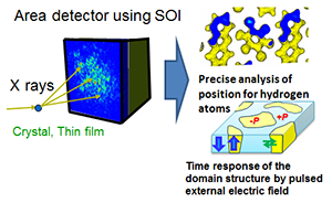
High spatial resolution is required to identify neighboring diffraction images accurately and to downsize the detector that are placed in a vacuum chamber to measure soft X-rays. Using the technology of SOI (silicon on insulator) wafers, which enables integration of the X-ray sensor part with the signal-processing circuit through the oxide layer, it is possible to enhance the definition of an image with a pixel size <50 μm. Since the study of the change of material structure with time by stimulating a sample from outside is essential for the development of new electronics materials, we need to increase the speed at which the image detector records data to <1 ms per frame. In 2013, the goal of the research project entitled "Imaging for the research of spatial hierarchical structures and dynamics by using synchrotron radiation," which started under the Grant in Aid for Scientific Research on Innovative Area, "Development of new quantum imaging explored by three dimensional semiconductor detectors," was to enable the consecutive recording of high-speed phenomena by using a pixel size of 30 μm and internal memory.

The development of an ultra-high-speed detector system in which a linear array of silicon avalanche photodiodes (Si-APD) is used as an X-ray sensor is underway. In the fall of 2012, we realized a time resolution of 1 ns with a 64-pixel array (pixel size = 200 100 μm2). This detector system can be used to measure physical properties by using nuclear resonant scattering and time-resolved measurements of X-ray diffraction intensity. The development of X-ray detectors, where Si-APD is used as a sensor, at the Photon Factory (PF); the development of ultra-high-speed ASICs (application-specific integrated circuits) by the electronics system group at the Institute of Particle and Nuclear Studies; and collaborative research using high-integration electronic circuit technology with an FPGA (field-programmable gate array) are ongoing.

A high-speed polarization switching experiment at PF BL-16A is underway. Auger electrons emitted from the surface of a sample irradiated by synchrotron radiation are detected with depth resolution by a 30-channel multi-anode microchannel plate (MCP). By 2010, we had measured X-ray magnetic circular dichroism (XMCD) by using high-speed polarization switching (10 Hz) and succeeded in measuring the X-ray absorption spectra from each detector channel. Since 2011, we have been working on a high-speed pulse system that can handle 104 counts per 1 ms. ASIC was chosen as the high-speed pulse amplifier; it is also used in the J-PARC muon μSR spectroscope system, designed by the E-sys group at the Institute of Particle and Nuclear Studies.
In addition, the development of a scanning transmission X-ray microscope system is underway at the PF, and we are collaborating with them as a working group.
Organization of the Photon Factory
BL-16A, BL-14A, BL-15A
IMSS Instrument R&D team: https://www2.kek.jp/imss/iird/ (Japanese only)
Open Source Consortium of Instrumentation (OSC) (Open-It): http://www-osc.kek.jp/ (Japanese only)
Ultra-fast signal processing system for two-dimentional pixel detectors (FPIX): http://rd.kek.jp/project/fpix/index_e.html
Grant-in-Aid for Scientific Research on Innovative Areas "Interdisciplinary research on quantum imaging opened with 3D semiconductor detector": http://soipix.jp/index_en.html