Development of TRHEPD: the ultimate tool for surface structure analysis
PressreleaseApril 22, 2014
Advanced Science Research Center, Japan Atomic Energy Agency
High Energy Accelerator Research Organization, KEK
A group led by principal researcher Atsuo Kawasuso of the Advanced Science Research Center, Japan Atomic Energy Agency, (JAEA), Professor Toshio Hyodo of the Institute of Materials Structure Science, KEK, and Professor Emeritus Ayahiko Ichimiya of Nagoya University has refined reflection high-energy positron diffraction (RHEPD) method to develop total-reflection high-energy positron diffraction (TRHEPD) method. A high-intensity positron beam whose intensity was increased 10 times in 2010 was used to obtain clear diffraction patterns from the (111) reconstructed surface of a silicon single crystal.
The structure of a solid surface at the atomic level can be analyzed using electron beam and X-ray diffraction patterns. However, when such beams are used, various measures are necessary to obtain information from the topmost layer only. On the other hand, for positrons with their positive charge, it is straightforward to obtain information only for the atomic arrangement on the topmost surface. That is, positrons incident on a surface at a glancing angle below a critical angle are totally reflected at the first atomic layer and do not enter the crystal at all. By using this characteristic of positron beams, diffraction patterns reflecting the atomic positions at the topmost surface can be obtained by directing positrons with a given energy at a certain grazing angle to the crystal surface. The diffraction patterns can then be used to determine the atomic positions at the topmost surface. This forms the essence of the TRHEPD method.
The silicon (111) topmost surface that was measured has a so-called reconstructed Si(111)-(7×7) DAS structure (Fig. 1), in which silicon atoms are reordered from the structure of the (111) planes inside the crystal. The 10-keV positrons used in the measurements are totally reflected when incident on the surface at a glancing angle below the critical angle of 2.0°. Therefore, the diffraction pattern at a glancing angle of 1.3° (Fig. 2) corresponds to the topmost atomic layer only, while that at a glancing angle of 2.1° includes reflections from the second atomic layer.
Comparisons between simulations (Fig. 3) show that the positron diffraction patterns corresponding to a glancing angle of 1.3° include information on the adatoms and the atoms at the first layer only, and that corresponding to a glancing angle of 2.1° includes information on the atoms on the second layer. Furthermore, similar comparison for electrons shows that they definitely penetrate below the second layer even at a glancing angle of 1.3°.
The results indicate that positrons penetrate less into crystals than electrons, and that diffraction patterns only from atoms exposed at the topmost surface can be obtained by using a glancing angle below the critical angle. By measuring the diffraction patterns obtained at increasing glancing angles, one obtains data with increasing contributions from lower atomic layers. These demonstrate that TRHEPD is very sensitive and useful for highly accurate analysis of the arrangements of atoms at the topmost surface and subsurface of solids.
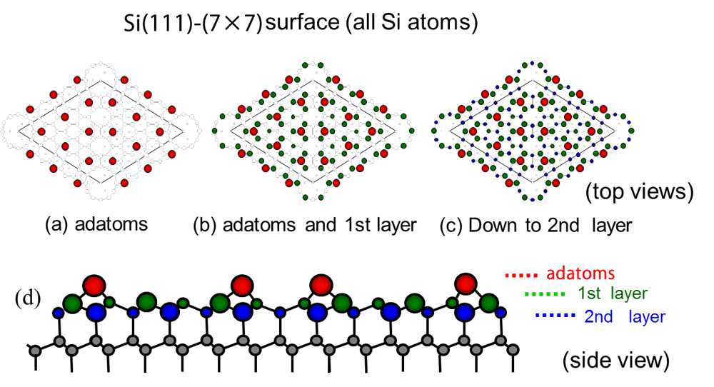 Fig. 1 Schematic diagram of Si(111)-(7×7) DAS (dimer-adatom-stacking-fault) structure. The circles are all silicon atoms.
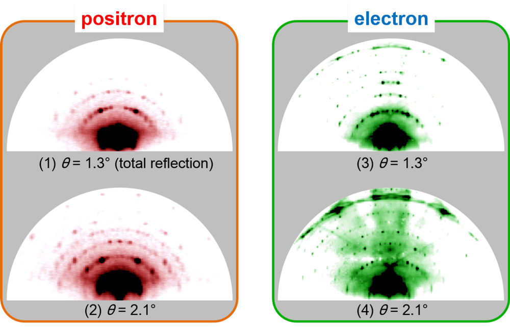 Fig. 2: Positron and electron diffraction patterns obtained for glancing angles of 1.3° and 2.1°.
The spots due to the symmetry of the atomic layers inside the crystal are visible on the periphery of the reflection high-energy electron diffraction (RHEED) patterns and the reflection high-energy positron diffraction (RHEPD) pattern at θ = 2.1°, but not in the RHEPD pattern at θ = 1.3° (TRHEPD pattern). The Kikuchi lines are much less prominent in the RHEPD patterns.
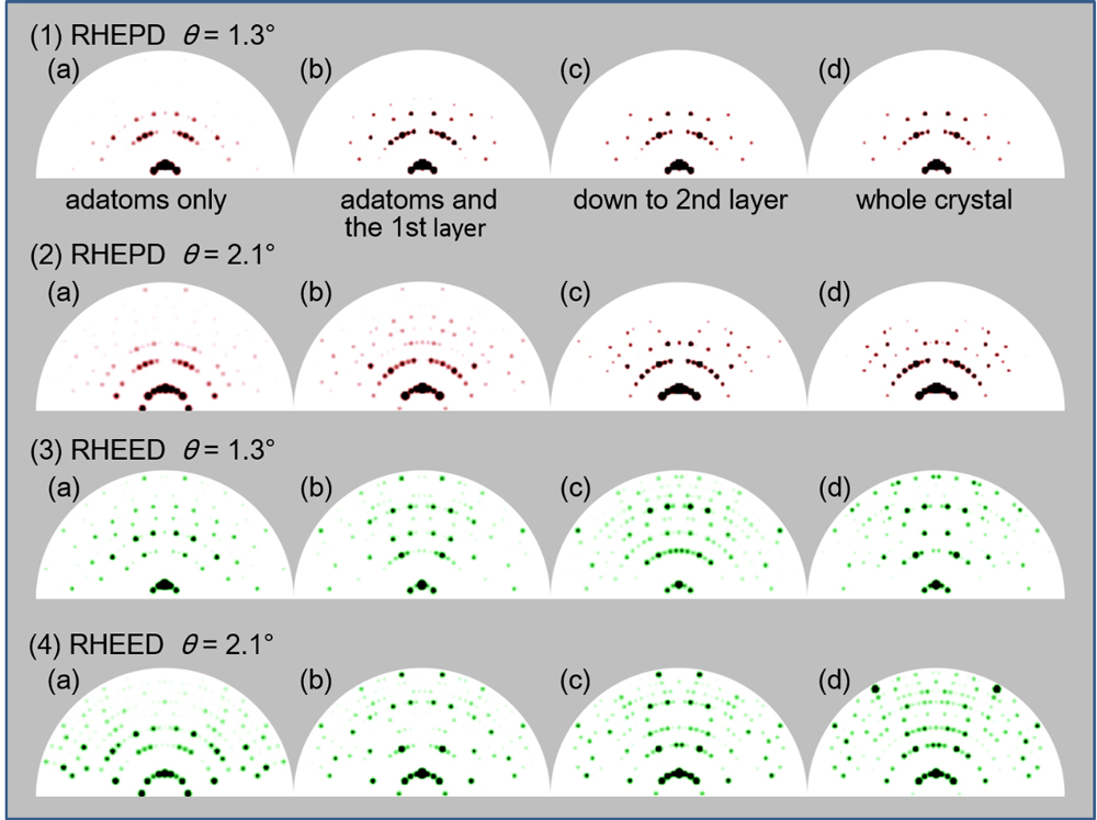 Fig. 3: Simulated diffraction patterns from the Si(111)-(7×7) surface
In (1), images (b), (c), and (d) are indistinguishable from each other, which indicates that the diffraction pattern from the entire crystal effectively contains information from the adatoms and first layer only.
In (2), there is a difference between (b) that contains information up to the first layer and (c) that contains information up to the second layer. As (c) and (d) are very similar, we can conclude that positrons reach the second layer for this glancing angle.
There are differences between (c) and (d) for a glancing angle of 1.3° for electrons, and therefore, we conclude that electrons penetrate below the second layer.
|
|
Media Contact
[ For Public Relations ]
Public Relations Office, Japan Atomic Energy Agency
TEL: +81-3-3592-2346
FAX: +81-3-5157-1950
Public Relations Office, High Energy Accelerator Research Organization (KEK), Japan
Saeko Okada
Senior Press Officer, Public Relations Office, KEK
TEL: +81-29-879-6046
FAX: +81-29-879-6049
E-mail: press@kek.jp
Related Link
Advanced Science Research Center, JAEA
Institute of Materials Structure Science(IMSS)
Photon Factory
Slow Positron Facility
Applied Physics Express
Related Issue
December 5, 2013 Press Release
Successful Determination of Silicene Structure Using Reflection High-Energy Positron Diffracion (RHEPD)
June 27, 2012 Press Release
Successful generation of a positronium beam that can be readily accelerated to over 1 keV
詳しくは下記のページをご覧ください
http://