The properties and functions of materials are closely related to the arrangement of the atoms that make up the materials, and the same is true for the atomic layered materials that appear on the surface. There have been few studies, however, on the close relationship between them on such materials. In this project, we will develop the infrastructure for multi-probe research to measure the atomic arrangement and electronic state/functions of the surface layer of materials, and will use data-driven science and fast computational techniques to elucidate the mechanisms of new functions in atomic layered materials. For example, we will contribute to the development of superconducting materials, nanotechnology materials, and catalytic materials for the realization of a super-smart and sustainable society.
WADA, Ken / MOCHIZUKI, Izumi / Rezwan AHMED / HYODO, Toshio / AMEMIYA, Kenta / MASE, Kazuhiko /
OZAWA, Kenichi / MIKAMI, Riki
JAEA, AIST, Waseda University, Osaka University, Kyushu University, Rikkyo University, QST, NIMS, NIFS, The University of Tokyo, Tokyo University of Science
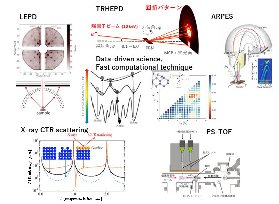
Total-reflection high-energy positron diffraction (TRHEPD),
Low-energy positron diffraction (LEPD),
X-ray CTR scattering,
Photoelectron spectroscopy,
positronium time-of-flight (Ps-TOF),
Data-driven science, fast computational technique