- Topics
MAPS Academy 2025 Held for Young Researchers
August 26th, 2025
-
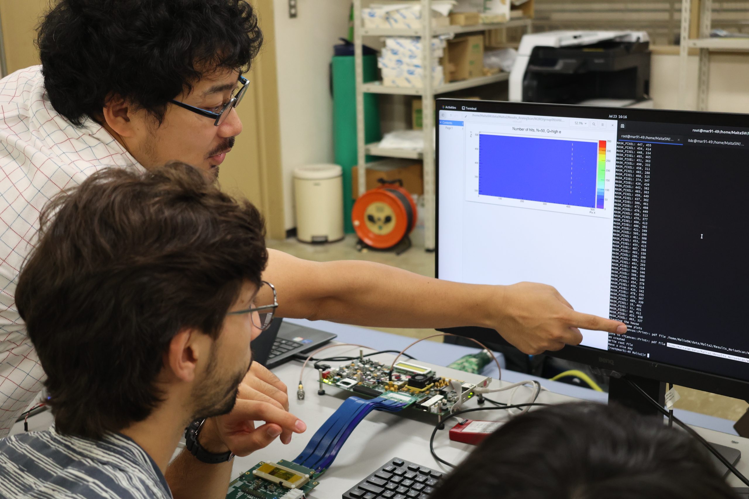
Hands-on training on the operating of MALTA, a radiation-tolerant MAPS sensor
The MAPS Academy 2025 took place at KEK Tsukuba Campus from July 23rd to July 30th, organized by KEK Institute of Particle and Nuclear Studies (IPNS).
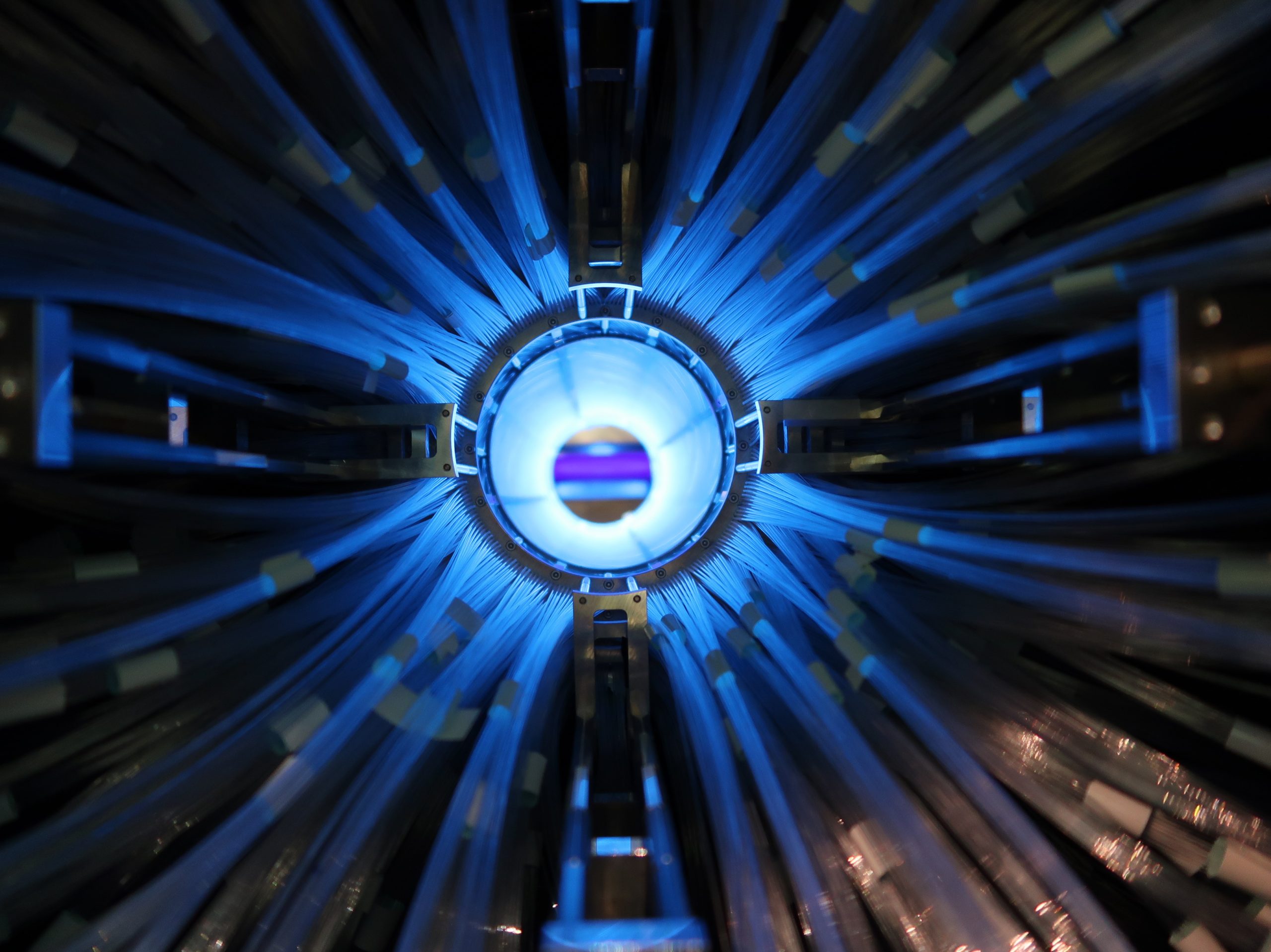
MAPS (Monolithic Active Pixel Sensors) is a semiconductor detector that utilizes CMOS technology, which combine the sensing element and readout electronics on the same device. MAPS attracts attention as a next generation sensor for its compact design, high-performance and cost-effective production. In future collider experiments, MAPS can be applied to a wide range of uses, including tracking detectors, calorimeters, and muon detectors.
MAPS Academy 2025 had an intensive program for young researchers to acquire fundamental knowledge and skills in designing and developing MAPS technologies. Centered on hands-on training in MAPS design and operation, the eight-day program also featured lectures ranging from basic principles of MAPS to the latest developments in the field. Twenty participants from diverse fields, including particle and nuclear physics as well as sensor engineering, were selected from a pool of applicants that was more than three times the number of available seats. With participants coming from around the world, the school had an international atmosphere, alongside ten lecturers in total, including six from France and Germany.
-
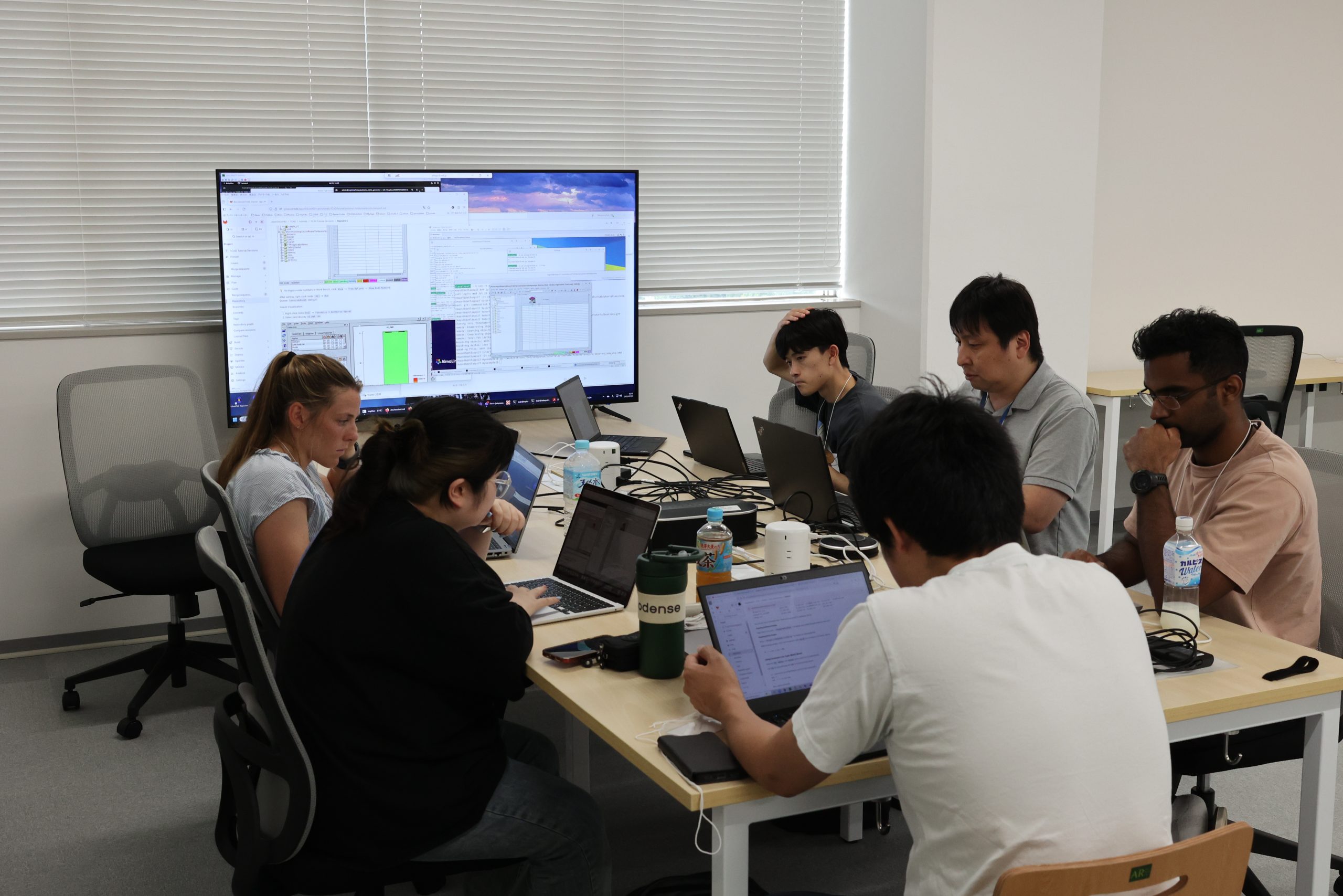
Hands-on session on TCAD simulations for calculating electric fields and charge collection efficiency in pixel sensors
Associate Professor Yuji Enari from the IPNS Instrumentation Technology Development Center (IDTC), one of the organizers, said: “This was the first school in the world dedicated to MAPS, and at first I was unsure how it would go. But thanks to the commitment of the lecturers and the enthusiasm of the participants, it turned out to be a truly wonderful eight days. We hope to build on this experience and further develop the program into a continuing series.”
-
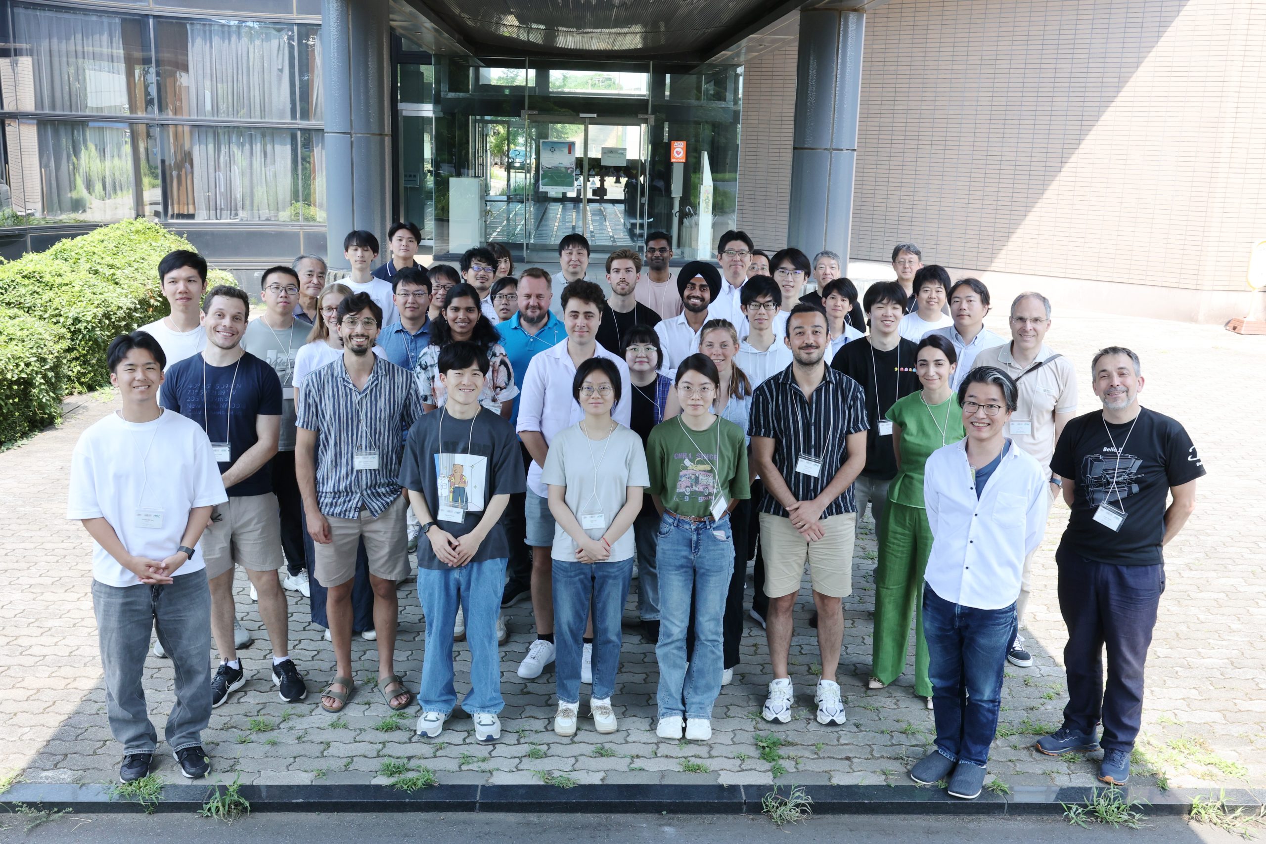
Group photo at the Building 3, taken on the first day (23rd July)